No etching, more precision: a simpler way to build brain interfaces
GA, UNITED STATES, August 1, 2025 /EINPresswire.com/ -- A new fabrication strategy for neural microneedle arrays is offering a cleaner, faster route to high-performance brain interfaces. This "local de-insulation" method allows researchers to precisely expose recording sites without the need for traditional etching, which often complicates production or damages electrode tips. Using a soft, elastic mask during insulation, the team achieved uniformly exposed tips with minimal residue. In both bench-top and animal studies, the resulting electrode arrays showed excellent signal clarity and structural reliability. This work opens the door to scalable, minimally invasive brain–machine interfaces that could transform neural recording technologies.
Silicon-based neural microneedle arrays remain essential in neuroscience and brain–machine interface research due to their ability to record highly localized electrical signals chronically. Unlike flat electrodes, microneedle arrays feature 3D tips that must be selectively exposed to function properly. However, conventional lithographic etching methods are often imprecise, time-consuming, and prone to damaging delicate needle structures. Prior attempts to improve tip exposure have included complex photoresist layers, manual trimming, or ion beam techniques—each with trade-offs in accuracy, speed, and uniformity. Due to these persistent limitations, there is an urgent need for a more reliable and scalable solution to prepare microneedle arrays for high-resolution neural recording.
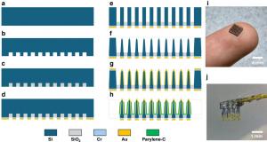
In a study published on May 26, 2025, in Microsystems & Nanoengineering, researchers from the Institute of Semiconductors, Chinese Academy of Sciences, unveiled a novel fabrication technique that simplifies the preparation of neural microneedle arrays. The “local de-insulation” method sidesteps traditional etching by applying a soft, thin film Polydimethylsiloxane (PDMS) mask during insulation, protecting the needle tips and ensuring consistent exposure. The technique demonstrated impressive results in both lab and live animal tests, suggesting a promising leap forward in the development of next-generation brain–computer interfaces.
At the core of the innovation is a simple yet effective idea: insert the microneedle array into a semi-cured PDMS layer before insulation. The elastic mask tightly wraps the electrode tips, preventing Parylene-C from depositing during the chemical vapor deposition process. When the array is withdrawn, the insulation layer naturally fractures at the interface, revealing clean, uniform tips. With optimized parameters—such as a 50 μm mask thickness and 3 μm insulation layer—the team achieved a tip exposure uniformity of just 2.32%, significantly better than earlier methods. After platinum black modification, the electrodes showed a low impedance of 33.2 kΩ and excellent biocompatibility. In rat models, 15 of 16 channels recorded strong neural spikes, with the best signal-to-noise ratio reaching 28.47. These results confirm not only the structural consistency of the arrays but also their high-fidelity signal performance in live tissue environments.
“We’ve demonstrated that high-precision neural electrodes don’t require complicated etching steps,” said Dr. Xin Zhao, lead author of the study. “Our approach offers a practical solution to a long-standing problem in neurotechnology fabrication. By protecting the needle tips during insulation rather than removing material afterward, we reduce damage and increase yield. This technique could pave the way for more accessible and scalable production of advanced neural interfaces.”
This de-insulation strategy holds significant promise for both research and clinical applications. Its speed and reliability make it ideal for manufacturing high-density electrode arrays used in neuroprosthetics, brain mapping, and chronic implants. With consistent tip exposure and robust electrochemical performance, the method enhances both recording quality and long-term stability. The research team aims to further refine the fabrication process for use in large-animal and human trials. As the demand for minimally invasive, high-resolution and chronicneural interfaces grows, this approach could play a pivotal role in bridging technology and the human brain.
References
DOI
10.1038/s41378-025-00922-6
Original Source URL
https://doi.org/10.1038/s41378-025-00922-6
Funding information
This work was supported by the National Natural Science Foundation of China under grant 62071447 and the National Key R&D Program of China under grant 2022YFF1202303.
Lucy Wang
BioDesign Research
email us here
Legal Disclaimer:
EIN Presswire provides this news content "as is" without warranty of any kind. We do not accept any responsibility or liability for the accuracy, content, images, videos, licenses, completeness, legality, or reliability of the information contained in this article. If you have any complaints or copyright issues related to this article, kindly contact the author above.

